Springer Nature
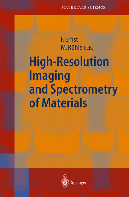
High-Resolution Imaging And Spectrometry Of Materials
Miglior prezzo disponibile
169,99$
Springer Nature · Spedizione gratuita
VISAPayPal
Prezzi aggiornati
Specifiche
MarcaSpringer Nature
CondizioneNuovo
Descrizione
The characterisation of materials and material systems is an essential aspect of materials science. A few decades ago it became obvious that, because the properties of materials depend so critically on the microstructure of their components, this characterisation must be determined to the atomic level. This means that the position - as well as the nature - of individual atoms has to be determined at "critical" regions close to defects such as dislocations, interfaces, and surfaces. The great impact of advanced transmission electron microscopy (TEM) techniques became apparent in the area of semiconducting materials, where the nature of internal interfaces between silicon and the corresponding silicides could be identified, and the results used to enhance the understanding of the properties of the compounds studied. At that time, advanced TEM techniques existed predominantly in the US. However, advanced TEM instrumentation was not available in the ma terials science and solid-state science communities in Germany. This gap was bridged by the late Peter Haasen who, after a visit to the US, initiated a Priority Programme on Microstructural Characterisation at the Volkswagen Foundation (Hannover). The programme was in effect from 1985 to 1997 and supported a wide range of research projects - from fundamental, trendy, innovative projects to projects in applied materials science.
Storico prezzi
Ricevi una notifica se il prezzo scende
Ti invieremo un'email quando il prezzo di questo prodotto diminuirà.
- Aggiornamenti dei prezzi in tempo reale
- Oltre 50 negozi monitorati
- Avvisi gratuiti di calo prezzo
- Solo negozi verificati
Avvisami quando il prezzo scende sotto: 169,99$
Prodotti simili
Una selezione di prodotti che potrebbero interessarti. Guarda tutti
 High-Resolution Imaging And Spectrometry Of Materials
169,99$
High-Resolution Imaging And Spectrometry Of Materials
169,99$
 Mass Spectrometry Imaging Of Small Molecules
109,00$
Mass Spectrometry Imaging Of Small Molecules
109,00$
 High-Resolution Imaging Of Cellular Proteins
84,99$
High-Resolution Imaging Of Cellular Proteins
84,99$
 High Resolution Imaging, Spectroscopy And Nuclear Quantum Effects Of Interfacial Water
109,99$
High Resolution Imaging, Spectroscopy And Nuclear Quantum Effects Of Interfacial Water
109,99$
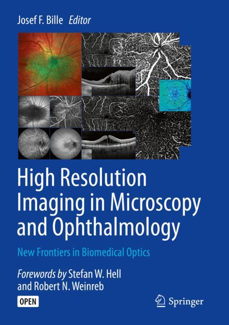 High Resolution Imaging In Microscopy And Ophthalmology
59,99$
High Resolution Imaging In Microscopy And Ophthalmology
59,99$
 High-Resolution Microwave Imaging
189,00$
High-Resolution Microwave Imaging
189,00$
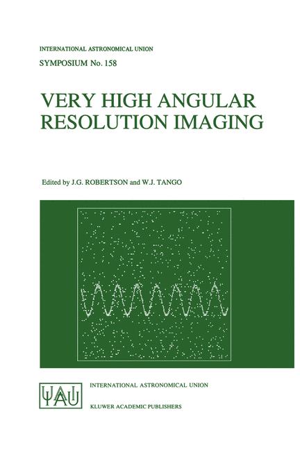 Very High Angular Resolution Imaging
219,99$
Very High Angular Resolution Imaging
219,99$
 Advanced X-Ray Imaging Of Electrochemical Energy Materials And Devices
179,99$
Advanced X-Ray Imaging Of Electrochemical Energy Materials And Devices
179,99$